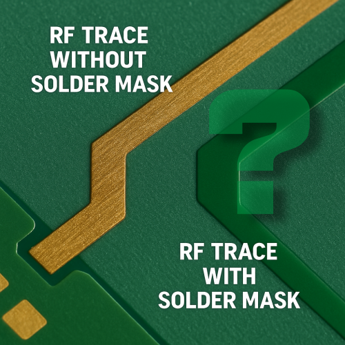
Removing Solder Mask on RF Traces
When designing RF PCBs, every small detail can have a significant impact on signal performance. One frequently debated practice is whether to remove solder mask over RF traces. Let’s explore…
When designing RF PCBs, every small detail can have a significant impact on signal performance. One frequently debated practice is whether to remove solder mask over RF traces. Let’s explore…

PCB Layout Good Practices: Designing for Performance and ReliabilityDesigning a printed circuit board (PCB) isn’t just about connecting components—it’s about creating a layout that’s functional, reliable, and manufacturable. Whether you're…

Copper is a crucial material in the manufacturing of printed circuit boards (PCBs) and other electronic components due to its excellent electrical conductivity. Two common types of copper foils used…
Printed Circuit Boards (PCBs) form the backbone of modern electronics, enabling intricate designs and high-speed signal transmission. Among the numerous techniques employed in PCB design, mitred traces are particularly noteworthy…

In the world of Printed Circuit Board (PCB) design, performance and precision are key. Every decision—from the type of symbols you use to how they’re implemented—can impact not only the…
Buying a digital product from our store is quick and easy. Just follow these simple steps:1. Browse Our Products Start by exploring our collection to find the digital item you’d…