Altium Library Creation

Uncategorized
Wishlist Share

About Course

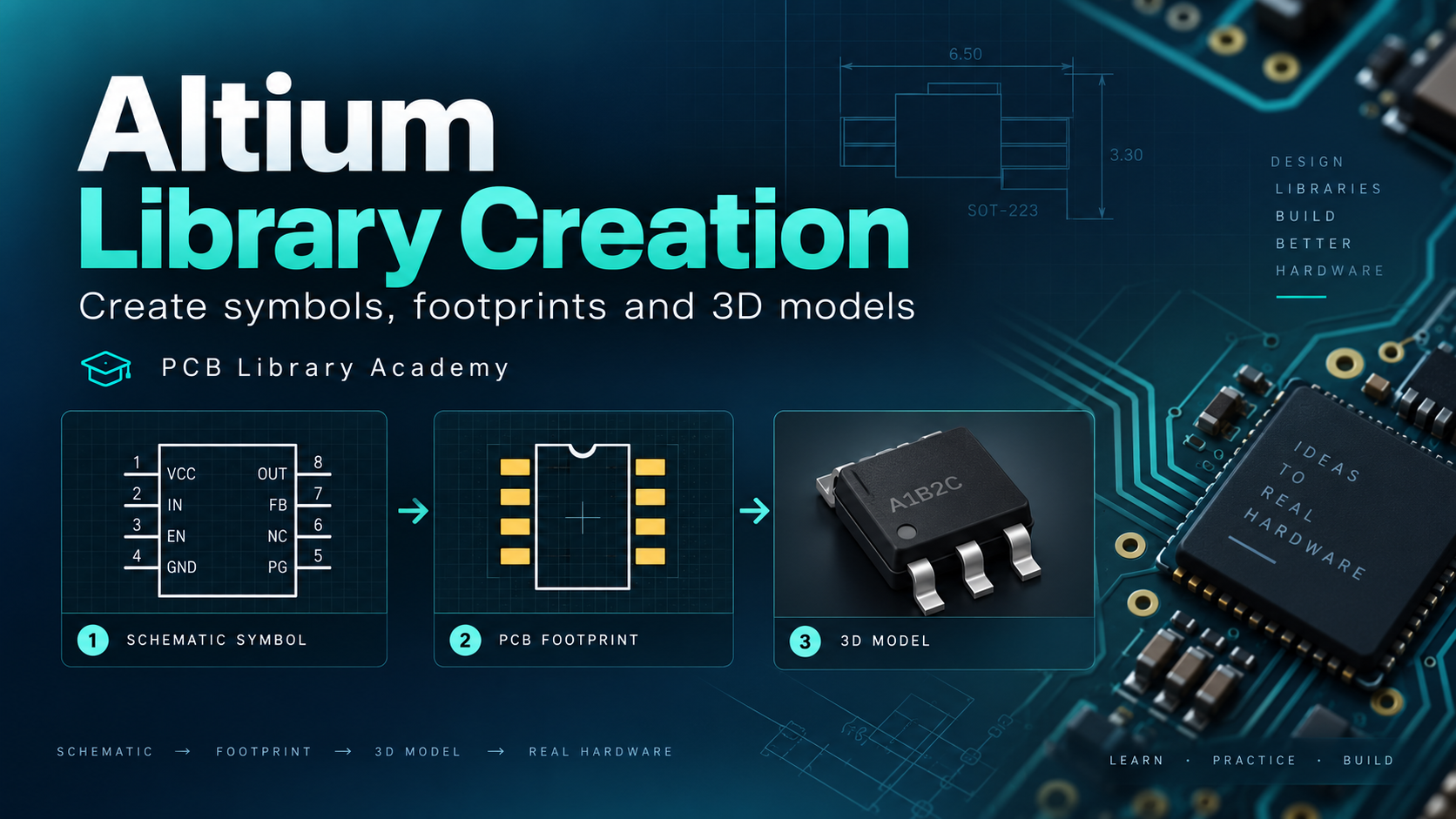
Learn how to create complete component libraries in Altium Designer, from the schematic symbol to the PCB footprint and 3D model.

In this course, you will work through the component creation process step by step using a real datasheet. You will learn how to create and configure schematic symbols, define pins and component parameters, build PCB footprints using manufacturer dimensions, link the schematic and PCB models, and add a STEP model for 3D verification.

The course also covers practical library organization and validation techniques to help you create components that are accurate, consistent, and ready to use in real PCB projects.

This course is ideal for PCB designers, electronics engineers, technicians, and students who want to improve their Altium Designer library creation workflow.

Show More

What Will You Learn?

  • How to create a schematic library in Altium Designer
  • How to create and configure schematic symbols and pins
  • How to create PCB footprints from datasheet dimensions
  • How to link schematic symbols to PCB footprints
  • How to add component parameters and manufacturer information
  • How to add and position a 3D STEP model
  • How to validate a complete component before use

Course Content

Topic 1 — Introduction
Course Overview Understanding Altium Libraries Schematic Library vs PCB Library

  • 01 – Introduction to Altium Library Creation
    00:00

Topic 2 — Creating the Schematic Symbol
Creating a New Schematic Library Creating a New Component Drawing the Schematic Symbol Adding and Configuring Pins Pin Electrical Types Component Designator and Comment Adding Component Parameters

Topic 3 — Creating the PCB Footprint
Creating a New PCB Library Reading Package Dimensions from a Datasheet Creating and Configuring Pads Pad Numbering and Pin Mapping Creating the Component Outline Adding Silkscreen Adding Mechanical Information Checking Dimensions and Origin

Topic 4 — Linking Symbol and Footprint
Adding the PCB Footprint to the Schematic Component Checking Pin-to-Pad Mapping Testing the Component in a Schematic Transferring the Component to a PCB

Topic 5 — Adding the 3D Model
Understanding 3D Bodies in Altium Adding a STEP Model Positioning and Rotating the STEP Model Checking Component Height Verifying the Component in 3D View

Topic 6 — Component Validation
Checking Symbol Accuracy Checking Footprint Dimensions Checking Pin and Pad Numbers Checking Silkscreen and Mechanical Layers Final 3D Verification Common Library Creation Mistakes

Topic 7 — Finalizing the Component
Naming Conventions Saving and Organizing Library Files Final Component Review Course Conclusion

Student Ratings & Reviews

No Review Yet
No Review Yet